Table of Contents >> Show >> Hide
- Why Webcam PCBs Are More Interesting Than They Look
- Visible Light Inspection: Helpful, But Not Magic
- X-Ray Inspection: The Board Becomes Transparent
- What X-Rays Can Reveal Inside A Webcam PCB
- Cheap Webcams: Engineering Marvels Or Tiny Compromises?
- Why PCB Inspection Matters Beyond One Webcam
- The Security Side: A Webcam Is Also A Networked Computer
- Lessons For Makers, Repairers, And Curious Humans
- Seeing Differently Changes How We Value Electronics
- Personal Experiences And Practical Reflections On Webcam PCB Inspection
- Conclusion
Most people look at a webcam and see a plastic pebble with a lens, a cable, and perhaps a tiny blue LED that says, “Congratulations, you are now in a meeting.” Electronics people, however, see a little mystery box. Inside that innocent camera is a layered city of copper roads, solder islands, silicon neighborhoods, and microscopic decisions made by engineers who probably drank too much coffee during the layout deadline.
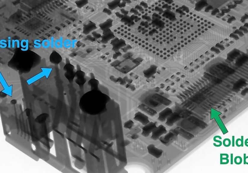
The title “Seeing A Webcam’s PCBs In A Whole Different Light” points to a wonderfully nerdy idea: what happens when we stop judging a printed circuit board only by what we can see on the surface? Under visible light, a cheap webcam PCB may look ordinary. Maybe a bit messy. Maybe a little too enthusiastic with the flux. But under X-ray inspection, the board becomes a transparent technical story. Hidden vias appear. Buried solder joints become visible. Ball grid array packages reveal their tiny solder spheres. Problems that would laugh at your desk lamp suddenly have nowhere to hide.
This is not just electronics eye candy. It is a practical lesson in how modern devices are built, why some gadgets fail early, and why inspection technology matters. A webcam may be small, cheap, and replaceable, but its circuit boards contain the same design challenges found in phones, routers, drones, security cameras, and countless connected devices. In other words, the humble webcam is a perfect classroomone that plugs into USB and occasionally makes your forehead look enormous.
Why Webcam PCBs Are More Interesting Than They Look
A webcam usually contains more than one printed circuit board, especially if it is a Wi-Fi security camera or a camera with night vision. One board may hold the main processor or system-on-chip. Another may carry the image sensor and lens assembly. A third may support the microphone, infrared LEDs, status LEDs, or power circuitry. On a cheap device, these boards may be compact, crowded, and connected with flexible cables, pin headers, castellated edges, or other cost-saving tricks.
At first glance, the board is just green, black, red, or blue fiberglass with shiny bits attached. But every piece has a job. Copper traces carry signals. Solder mask insulates and protects copper while leaving pads exposed for soldering. Vias act like tiny elevators, allowing signals to travel from one PCB layer to another. Components such as resistors, capacitors, crystals, regulators, memory chips, and processors work together to capture images, process video, move data, and power the whole operation without turning the device into a toaster.
Webcams are especially fun because they combine optics, electronics, firmware, and sometimes networking in a tiny package. The camera sensor turns light into electrical information. The processor compresses and manages that information. USB or Wi-Fi circuitry sends it outward. Infrared LEDs may help the camera see in the dark. A microphone may add audio. Suddenly, that five-dollar plastic eyeball looks less like a throwaway gadget and more like a miniature robot with a suspiciously busy social life.
Visible Light Inspection: Helpful, But Not Magic
The classic inspection method is the trusty “Mark I eyeball,” ideally upgraded with a magnifier, microscope, or macro camera. Visual inspection is still valuable. It can reveal crooked components, obvious solder bridges, missing parts, overheated areas, cracked connectors, residue, corrosion, damaged pads, and suspicious blobs that look like the board sneezed molten metal.
For hand soldering and repair, visible inspection is often enough to catch common issues. A good solder joint should be smooth, properly wetted, and mechanically stable. A bad joint may look dull, lumpy, cracked, or starved of solder. Too much solder can create bridges between pins. Too little solder can cause intermittent connections. Flux residue can be harmless in some cases, but excessive residue may suggest rushed manufacturing or poor cleaning.
The problem is that modern electronics are no longer designed with every joint visible. Many important solder connections are hidden underneath packages. Ball grid arrays, chip-scale packages, and some leadless components place their contacts below the component body. A microscope can admire the package from the outside all day, but it cannot see through the package and board. That is where visible light politely steps aside and X-ray inspection enters wearing a lab coat.
X-Ray Inspection: The Board Becomes Transparent
X-ray inspection works because different materials absorb X-rays differently. Dense materials such as solder and metal features show up strongly, while fiberglass and plastic are more transparent. For PCB inspection, this makes it possible to look beneath components, inside plated through holes, through multilayer structures, and under packages where the most interesting trouble often lives.
In an X-ray view of a webcam PCB, a BGA chip can look like a neat constellation of solder balls. Vias appear as rings or dots. Traces and copper pours form pale geometric patterns. Through-hole solder fill can be evaluated. Hidden defects such as voids, insufficient solder, bridges, and misaligned features can become visible. It is like giving the PCB a medical scan, except the patient is a camera and the diagnosis may be “needs better reflow.”
This matters because hidden defects can be sneaky. A board may power on during factory testing, ship to a customer, and work for weeks before heat, vibration, or thermal cycling exposes a weak solder joint. A tiny void in a solder ball may not cause immediate failure, but excessive voiding can reduce mechanical strength and affect heat transfer. A marginal via may behave until the device warms up. A poorly filled through-hole may pass casual inspection but fail when stressed. Electronics can be dramatic that way.
What X-Rays Can Reveal Inside A Webcam PCB
1. BGA Solder Ball Quality
Ball grid array packages are common in compact electronics because they allow many connections beneath a chip. That density is wonderful for design and terrible for eyeballs. With X-ray inspection, each solder ball can be checked for shape, spacing, voids, missing connections, and bridges. In a webcam, the main processor or memory package may use this kind of hidden connection. If one ball is poorly formed, the whole device can become a tiny paperweight with a lens.
2. Via And Through-Hole Problems
Vias are small plated holes that connect PCB layers. In multilayer boards, they are essential. X-ray imaging can reveal whether vias and through-holes are properly formed, filled, or aligned. A webcam PCB may use vias to route signals from the image sensor, processor, memory, power rails, and radio circuitry. When those tiny copper elevators fail, signals get stuck between floors.
3. Solder Bridges And Shorts
A solder bridge is an unwanted connection between pads or pins. Under visible light, bridges between exposed pins can often be spotted. Under hidden packages, however, bridges can be invisible without X-ray inspection. In a compact webcam, where low-cost assembly may push tolerances, hidden bridges can cause power faults, communication errors, or unpredictable behavior.
4. Insufficient Solder And Open Joints
Too little solder can produce a weak or incomplete electrical connection. X-ray inspection can show areas where solder did not properly wet the pad or component. This is especially useful for leadless parts and BGAs. A webcam that randomly disconnects, freezes, or refuses to boot may be suffering from an invisible joint that looks fine from the outside.
5. Component Structure And Counterfeit Clues
X-rays can also reveal internal package structures. For engineers and failure analysts, this can help compare components, inspect bond wires, identify cracked packages, or detect suspicious construction. While a casual hobbyist probably will not X-ray every bargain-bin webcam, the method shows how much information is hidden inside ordinary electronics.
Cheap Webcams: Engineering Marvels Or Tiny Compromises?
The answer is yes. Cheap webcams are both impressive and compromised. They pack image capture, processing, power regulation, communication, audio, and sometimes night vision into a product that may cost less than lunch. That is not easy. The fact that these devices work at all is a minor miracle of modern manufacturing.
But low cost often means trade-offs. Boards may be thin. Cleaning may be minimal. Connectors may be fragile. Shields may be absent. Cables may be barely long enough to survive assembly. Soldering may be adequate rather than beautiful. The mechanical design may depend on hot glue with the confidence of a bridge engineer. None of this automatically means the product is bad, but it does mean inspection can reveal a lot about priorities.
For example, visible inspection might show leftover flux, uneven hand-soldered LEDs, or slightly crooked connectors. X-ray inspection might reveal more serious hidden issues: questionable via fill, insufficient solder in through-holes, or voiding under a chip. The outside of a board can be merely untidy, while the inside tells the real story. Electronics, like people before their first coffee, should not be judged only by surface appearance.
Why PCB Inspection Matters Beyond One Webcam
PCB inspection is not just for engineers with expensive machines. It affects everyone who buys electronics. A better-inspected board is more likely to survive shipping, heat, vibration, long operating hours, and the occasional user who plugs it in upside down with heroic determination.
In manufacturing, inspection helps catch problems before products leave the factory. Automated optical inspection can check visible components quickly. Solder paste inspection can verify paste deposits before reflow. X-ray inspection can evaluate hidden joints after assembly. Functional testing confirms that the device actually works. These methods complement one another because no single inspection technique catches everything.
For high-reliability electronicsmedical devices, aerospace systems, automotive modules, industrial controlsthe stakes are much higher than a glitchy webcam. Hidden solder defects can lead to expensive failures or safety risks. That is why workmanship standards, process control, and non-destructive testing matter. A webcam teardown is fun; the underlying inspection lesson is serious.
The Security Side: A Webcam Is Also A Networked Computer
If the webcam is a simple USB model, its main job is to send video to a host computer. If it is a Wi-Fi camera, it becomes a networked device with firmware, credentials, cloud services, and security responsibilities. That changes the conversation. The PCB may show the hardware story, but the software and network behavior tell another one.
Connected cameras have a long history of security concerns, especially when users keep default passwords, skip firmware updates, expose devices directly to the internet, or buy products with poor long-term support. A cheap Wi-Fi camera may contain perfectly reasonable hardware but still be risky if its software is careless. The board can be soldered beautifully and still make terrible cybersecurity decisions. Apparently, even circuit boards can have trust issues.
Practical advice is simple: change default passwords, use strong unique credentials, apply firmware updates, place cameras on a separate network when possible, disable features you do not use, and avoid exposing camera interfaces directly to the public internet. Seeing a webcam’s PCB in a different light should also remind us to see the whole product differentlyas hardware, software, supply chain, and privacy device all at once.
Lessons For Makers, Repairers, And Curious Humans
You do not need an X-ray machine to learn from this kind of teardown. A basic visual inspection can still teach a lot. Open a retired webcam and look at the layout. Find the image sensor. Identify the crystal oscillator. Trace the USB connector or Wi-Fi module. Notice how the infrared LEDs are arranged. Look for test pads, programming headers, unpopulated footprints, and manufacturing marks. Those small details reveal how products are designed for assembly, testing, and cost control.
If you repair electronics, the lesson is even more direct: not every failure is visible. When a board looks perfect but behaves badly, hidden joints, cracked vias, damaged internal layers, or package-level defects may be involved. Reflowing, probing, thermal testing, continuity checks, and careful observation can help, but some problems remain stubborn without advanced tools.
For PCB designers, the webcam is a reminder to design for inspection and reliability. Leave useful test points. Avoid unnecessary density when space allows. Think about thermal paths. Use appropriate via structures. Follow solder mask and pad design recommendations. Remember that the cheapest layout is not always the cheapest product if it increases failures, returns, or support headaches.
Seeing Differently Changes How We Value Electronics
The best part of X-raying a webcam PCB is not just the cool image. It is the shift in perspective. A device that seemed simple becomes layered and complex. A cheap board becomes a manufacturing case study. A solder blob becomes evidence. A via becomes a design decision. A hidden BGA joint becomes a potential point of failure or proof of good process control.
That perspective makes electronics more interesting and, frankly, more respectable. Modern gadgets are often treated as disposable, but even inexpensive devices contain remarkable engineering. They are the result of material science, optical design, PCB fabrication, assembly automation, firmware, logistics, and cost optimization. Seeing the inside helps us appreciate the outside.
It also encourages better habits. We become more willing to repair instead of replace. We become more skeptical of suspiciously cheap connected devices. We learn to inspect our own soldering more carefully. We understand why hidden defects matter. And we gain a deeper respect for the invisible work that keeps electronics running.
Personal Experiences And Practical Reflections On Webcam PCB Inspection
Working with small camera boards teaches patience very quickly. The first thing you notice is that everything is smaller than your confidence. Screws vanish. Ribbon cables behave like emotional spaghetti. Connectors look sturdy until you touch them, at which point they reveal they were apparently designed by someone who hates repair technicians. Still, taking apart a webcam is one of the best beginner-friendly ways to understand compact electronics.
One practical experience many hobbyists share is discovering that a “dead” webcam is not always dead. Sometimes the problem is mechanical: a broken USB cable, cracked solder around the connector, or a loose internal ribbon. A careful inspection under magnification can reveal lifted pads, cold joints, or a connector that wiggles when it should not. In those cases, a simple repair may bring the camera back to life. The repair feels heroic, even if the patient is a plastic camera worth less than the solder wick.
Another common experience is realizing how much lighting changes what you see. Straight overhead light can hide defects because it flattens the board visually. Oblique light from the side can reveal cracks, texture, flux residue, and solder shape. A cheap USB microscope with adjustable LEDs can make a board look entirely different. Rotate the PCB, change the angle, and suddenly a suspicious joint becomes obvious. This is the visible-light version of the article’s larger message: different light reveals different truths.
When inspecting webcam PCBs, it helps to create a simple routine. First, check the connectors and cables because they suffer the most handling stress. Second, inspect power-related components such as regulators, diodes, and capacitors. Third, examine the sensor board and lens area for dust, corrosion, or physical damage. Fourth, look for heat discoloration or cracked solder near larger parts. Finally, check the board for test pads and labels that may help identify voltage rails or communication lines.
The most humbling experience is when everything looks perfect and the board still refuses to work. That is where the “whole different light” idea becomes more than a phrase. Some defects are internal. Some are under packages. Some are firmware-related. Some are caused by electrostatic damage or a component failure that leaves no visible mark. At that point, an X-ray system, thermal camera, oscilloscope, or logic analyzer can reveal what the eye cannot. The board is not being mysterious for fun; it is simply speaking a language that requires better tools.
For makers designing their own camera projects, the experience also teaches respect for layout. Image sensors can be sensitive to noise. High-speed USB traces deserve care. Power rails need decoupling. LEDs need proper current control. Mechanical alignment matters because the lens and sensor must sit correctly. A camera PCB is not just a place to glue components; it is a coordinated system where optics, electricity, heat, and mechanics all argue until the engineer makes peace.
Finally, opening and inspecting a webcam changes your relationship with everyday technology. The next time a tiny camera sits on top of a monitor, it no longer looks boring. It looks like a stack of design choices hidden behind plastic. Somewhere inside are copper traces, vias, solder joints, a sensor, a clock source, and a processor doing a surprisingly complicated job. Seeing those PCBs in a different light is not only about X-rays. It is about curiositythe kind that turns ordinary gadgets into tiny engineering stories worth reading.
Conclusion
Seeing a webcam’s PCBs in a whole different light is more than a clever teardown theme. It is a reminder that modern electronics hide their most important details beneath surfaces, packages, and layers. Visible inspection can catch many problems, but X-ray inspection reveals the secret life of solder joints, vias, BGA packages, and internal board structures. For manufacturers, that means better quality control. For repairers, it explains why some faults refuse to show themselves. For makers, it offers design lessons about testability, reliability, and layout discipline.
A webcam may be small, cheap, and easy to ignore, but inside it is a compact lesson in electronics manufacturing. Look closely enoughor shine the right kind of lightand the board stops being a green rectangle and starts becoming a map. And like any good map, it shows where the connections are, where the risks hide, and why the journey from “it works” to “it works reliably” is far more interesting than it looks.